Semiconductors are materials that have conductivity levels between conductors (which allow easy flow of electricity) and insulators (which block electricity). There are two main types: intrinsic, which occur naturally, and extrinsic, which are modified with impurities. Extrinsic semiconductors are divided into N-type (with extra electrons) and P-type (with extra “holes” or spaces for electrons).
The P-N junction forms where the P-type and N-type semiconductors meet. This junction has unique properties and plays a crucial role in electronic devices. Let’s delve deeper into understanding the P-N Junction in this discussion.
P-N Junction Definition:
A P-N junction serves as a boundary between two types of semiconductor materials: the p-type and the n-type, within a semiconductor.
Formation of P-N Junction:
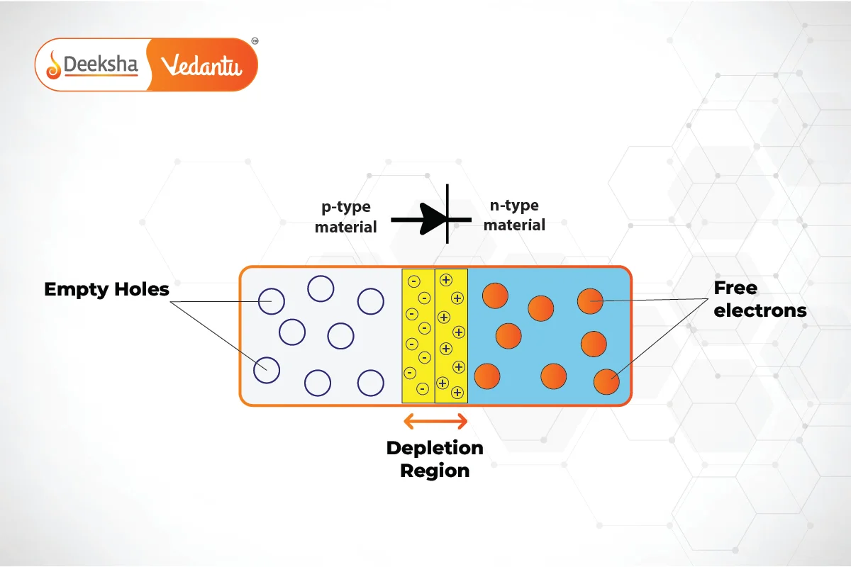
In a semiconductor, the P-N junction is established through a process called doping. The p-side (positive side) of the semiconductor contains an excess of “holes,” while the n-side (negative side) has an excess of electrons. Doping involves adding impurities to create this imbalance.
To overcome grain boundaries that hinder electron movement between different semiconductor materials, doping is used. For instance, imagine a thin sheet of p-type silicon semiconductor. By introducing a small amount of pentavalent impurity, part of the p-type silicon transforms into n-type silicon. This creates a sheet with both p-type and n-type regions, forming a junction between them.

Processes at the P-N Junction:
After forming the P-N junction, two processes occur: diffusion and drift. Due to the difference in hole and electron concentrations on either side of the junction, holes diffuse from the p-side to the n-side, and electrons diffuse from the n-side to the p-side, resulting in a diffusion current.
As electrons move from the n-side to the p-side, ionized donors are left behind on the n-side, creating a positive charge layer. Similarly, when holes move from the p-side to the n-side, ionized acceptors are left behind on the p-side, forming a negative charge layer. This creates a depletion region with positive and negative charges on either side of the junction.
An electric field is generated due to this charge imbalance, directing from positive to negative charges. This electric field causes electrons on the p-side to drift towards the n-side, resulting in drift current. Interestingly, the direction of drift current opposes that of diffusion current.
P-N Junction Diode Biasing Conditions
The P-N junction diode operates in two regions: the P-type and the N-type. Depending on the voltage applied, there are three biasing conditions for the P-N junction diode:
Zero Bias: No external voltage is applied to the P-N junction diode. It operates under equilibrium without any external influence.
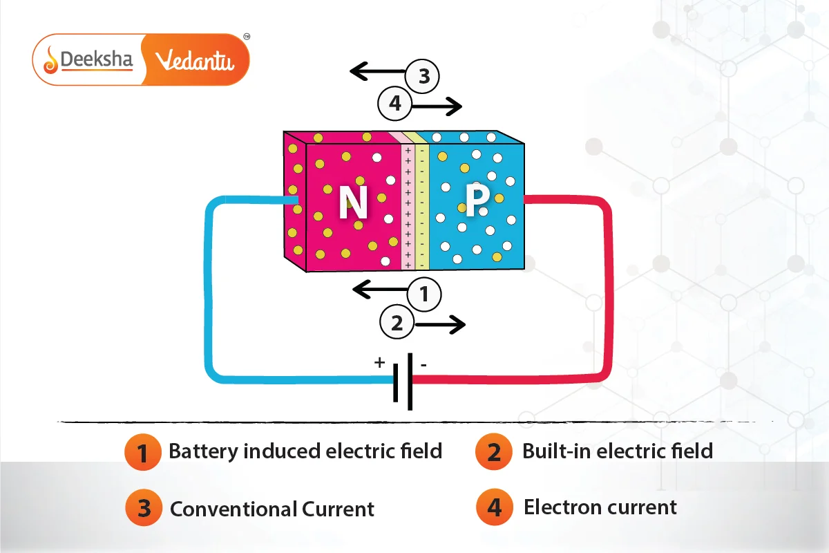
Forward Bias: The positive terminal of the voltage potential is connected to the P-type region, while the negative terminal is connected to the N-type region. This forward biasing allows current to flow through the diode easily.
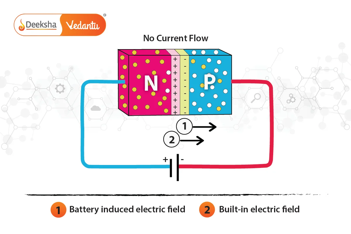
Reverse Bias: The negative terminal of the voltage potential is connected to the P-type region, and the positive terminal is connected to the N-type region. In this reverse biasing condition, the diode restricts current flow, and only a small leakage current may occur.
Forward Bias
When the positive terminal of the battery is connected to the p-type region and the negative terminal to the n-type region, the P-N junction is forward-biased. In this condition, the built-in electric field at the P-N junction and the applied electric field oppose each other. As a result, the combined electric field is weaker than the built-in electric field, leading to a thinner and less resistive depletion region.

As the applied voltage increases, the resistance of the depletion region decreases. In silicon, at around 0.6 volts, the resistance of the depletion region becomes negligible, allowing current to flow through the junction unimpeded.
Reverse Bias
When the negative terminal of the battery is connected to the p-type region and the positive terminal to the n-type region, the P-N junction is reverse biased. In this scenario, the built-in electric field and the applied electric field align in the same direction. Consequently, when these two fields are combined, the resultant electric field reinforces the built-in electric field, leading to the formation of a thicker and more resistive depletion region.

As the applied voltage increases, the depletion region becomes even more resistive and thicker. This is because the applied electric field strengthens the built-in electric field, intensifying the barrier to current flow across the junction.
P-N Junction Formula
The formula used to calculate the built-in potential difference across the P-N junction is given as:
Where:
is the built-in potential difference
is Boltzmann’s constant
is the temperature in Kelvin
is the charge of an electron
and
are the impurity concentrations of the P and N regions, respectively
is the intrinsic concentration of charge carriers.
PN junction diode – current flow
Current flow in a PN junction diode occurs due to the movement of charge carriers, namely electrons and holes, across the junction. When voltage is applied to the diode, electrons in the n-type region move towards the positive terminal (p-side), while holes in the p-type region move towards the negative terminal (n-side). This movement creates a concentration gradient between the two sides of the junction.
As a result of this concentration gradient, charge carriers flow from regions of higher concentration to regions of lower concentration. This movement of charge carriers inside the PN junction constitutes the current flow in the circuit. In essence, the flow of electrons and holes across the junction enables the passage of electric current through the diode.
V-I Characteristics of P-N Junction Diode

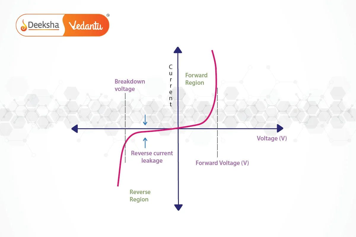
The V-I (voltage-current) characteristics of a P-N junction diode are represented by a curve plotting voltage on the x-axis and current on the y-axis. This curve illustrates three distinct regions of diode operation:
- Zero Bias:
In this state, no external voltage is applied, and the potential barrier at the junction prevents current flow. - Forward Bias:
Here, the p-type semiconductor is connected to the positive terminal, and the n-type to the negative terminal of an external voltage source. This reduces the potential barrier, enabling current flow. For silicon diodes, the barrier decreases at around 0.7 volts, and for germanium diodes, at around 0.3 volts. Initially, current increases gradually in the forward-biased region, resulting in a non-linear curve as the voltage surpasses the barrier. Once the barrier is overcome, the diode behaves normally, and current rises sharply with increasing voltage, resulting in a linear curve. - Reverse Bias:
In this configuration, the p-type semiconductor is connected to the negative terminal, and the n-type to the positive terminal of the external voltage source. This increases the potential barrier, restricting current flow. Initially, a reverse saturation current flows due to minority carriers present in the junction. As voltage is further increased, minority carriers gain kinetic energy, affecting majority carriers. At a certain point, the diode may experience breakdown, leading to potential damage if exceeded.
P-N Junction Diode Applications
The P-N junction diode finds various applications due to its unique properties:
- Photodiode:
When reverse biased, the diode becomes sensitive to light and can be used as a photodiode for light detection and sensing applications. - Solar Cell:
P-N junction diodes are utilized in solar cells to convert light energy into electrical energy efficiently. - LED Lighting:
When forward biased, the diode emits light and is commonly used in LED lighting applications for illumination purposes. - Rectification:
In electric circuits, P-N junction diodes act as rectifiers, converting alternating current (AC) into direct current (DC) by allowing current flow in only one direction. - Varactors:
P-N junction diodes function as voltage-controlled oscillators in varactors, where their capacitance varies with the applied voltage, enabling frequency modulation in electronic circuits.
FAQs
A concave mirror is a curved mirror with a reflecting surface that curves inward, resembling the inner surface of a hollow sphere.
Temperature affects the conductivity and mobility of charge carriers in a semiconductor, thereby influencing the electrical characteristics of a P-N junction device. In general, higher temperatures lead to increased conductivity and current flow.
The depletion region is a region near the junction where charge carriers are depleted due to the combination of majority carriers from both sides. It plays a crucial role in determining the electrical behavior of the junction.
P-N junctions are used in various electronic devices, including diodes, transistors, photodiodes, solar cells, LED lighting, rectifiers, and varactors.
In forward bias, the diode conducts current easily as the external voltage reduces the potential barrier at the junction. In reverse bias, the diode blocks current flow due to the increased potential barrier, except for a small reverse saturation current.
The operating regions of a P-N junction diode are zero bias, forward bias, and reverse bias. These conditions determine the behavior of the diode with respect to current flow and voltage applied.
A P-N junction is typically formed through a process called doping, where specific impurities are introduced into a semiconductor material to alter its electrical properties and create regions of excess positive and negative charge carriers.
A P-N junction is the boundary interface between a p-type semiconductor (with excess positive charge carriers) and an n-type semiconductor (with excess negative charge carriers) within a semiconductor device.
Related Topics
- Projectile Motion
- Electric Power
- Thermodynamics
- Energy
- Laws of Motion
- Mirrors
- Compound Microscope
- Noise Pollution
- Fleming’s Left-Hand Rule and Right-Hand Rule
- Protection Against Earthquake
- Kirchhoff’s Law
- Electricity
- Reflection Of Light
- Dispersion Of White Light By A Glass Prism
- The Human Eye And The Colourful World


![Rendered by QuickLaTeX.com \[V_{bi} = \frac{kT}{q} \ln \left( \frac{N_A \cdot N_D}{n_i^2} \right)\]](https://deekshalearning.com/wp-content/ql-cache/quicklatex.com-85433f645a53ca8752e68c691af323d1_l3.png)


Get Social